This section offers basic knowledge and glossary terms related to analog I/O, A/D conversion, and D/A conversion in an easy-to-understand way that includes illustrations. The content offered here is recommended knowledge for anyone looking to perform measurement control using a computer as well as anyone considering automating data logging or measurements. It may also prove a useful resource for individuals already using CONTEC analog I/O devices.
Contents
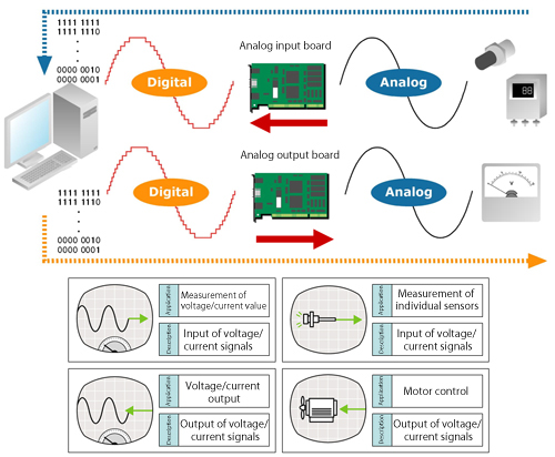
What is analog I/O?
The signals from sensors that measure surrounding natural factors such as temperature, pressure, and flow rate are often analog signals, and most control actuators move according to analog signals. On the other hand, only digital signals can be handled by computers. For this reason, in order to input a signal from a sensor using a computer, or to output a signal to an actuator, it's necessary to have a device that can bridge the analog signal and the digital signal handled by the computer. That bridge is called an analog I/O interface.
Analog I/O (Multi-function DAQ)
Analog I/O device classification
Analog input device(A/D conversion)
This device is responsible for converting analog signals from external devices to digital signals that can be processed by a computer.
Analog output device(D/A conversion)
This device converts the digital data from a computer to an analog signal before outputting that signal to an external device.
Analog I/O device(A/D, D/A conversion)
Analog I/O devices are devices with both an A/D conversion function and a D/A conversion function.
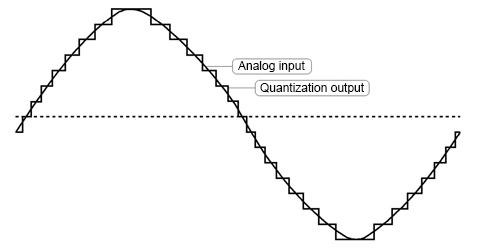
Analog to digital, digital to analog.
When inputting an external analog quantity into a computer, in order to display the quantity properly digitally, an infinite number of digits is need for the corresponding digital quantity. This is not possible with a computer capable of handling only a limited number of digits, even from the viewpoint of the circuit technology that makes up the converter.
The most effective way to solve this problem is to keep the number of digits within the acceptable range by rounding or using either the floor or the ceiling. In other words, this means replacing an amount within a certain range with a representative value. This is referred to as quantization.
When quantizing analog values represented by a solid line, you get a stepped line. This makes it possible to express any analog signal using a finite value. This technology is active in things many people are familiar with, for example, in cellular phones. Cell phones make calls by converting voices (analog) to digital sounds.
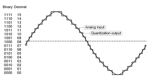
For example, the following figure shows a staircase in decimal numbers with the first step as 1, as well as the result if the decimal numbers are replaced with binary numbers. In this way, an analog quantity can be digitalized at 4 bits. This is the basic idea behind quantizing analog quantities.
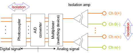
Analog I/O device isolation types
Analog I/O devices can be broadly classified into two categories: isolated and non-isolated. Let's look at the features of two types of isolation. Note that non-isolated types do not employ an isolation element.
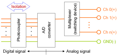
Bus isolation
Using a photocoupler, the computer and external I/O circuits are isolated. Because it's possible to prevent electrical interference from being introduced, this method allows for worry-free usability even if noise is easily generated in the wiring or if there is a concern of the computer malfunctioning or becoming damaged.
Independent (channel-to-channel) isolation
In addition to bus isolation, independent isolation uses a photocoupler and an isolation amplifier to add isolation between each input/output channel. This allows interference between channels to be prevented and allows for accurate sampling even if the equipment connected to the various channels have different ground levels.
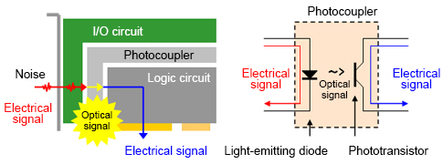
What is a photocoupler?
A photocoupler is a device that contains a light-emitting diode coupled to a phototransistor. The light-emitting diode outputs light when exposed to an electrical current (about 10 mA). The phototransistor receives this light, which turns the phototransistor ON, which results in an electrical current. Part of this optical signal is electrically insulated from the outside.
What is No. of I/O channels?
Input/output channels refer to the number of signals that can be input or output for a single device. In other words, this shows how many sensors (signal sources) or actuators (controlled objects) can be connected. In the specifications found in catalogs and the like, you may find expressions like X number of single-ended channels or X number of differential channels.
What is single-ended input?
Single-ended input, which uses a signal wire and a ground wire for a two-wire connection, is a method of measuring the voltage of a signal source using the potential difference from ground. For analog input, this is the most common input method and has the advantage of using only two lines for any one signal source. Compared with a differential input, a disadvantage of single-ended input is that it is easily affected by noise.
What is differential input?
Differential input uses two signal wires and a ground wire for a total of three wires for measuring the voltage of a signal source. The signal source potential (A–B) is measured by taking the difference in potential between ground and point A and between ground and point B. In this way, the noise from the ground is cancelled for A–B, which gives differential input the advantage of less susceptibility to noise compared to single-ended input. However, one disadvantage is that three wires are needed for one signal source, meaning that the number of channels that can be used is half that compared with single-ended input.
Analog I/O Input Channels (Multi-function DAQ)
Analog I/O Input Channels
Analog I/O Output Channels (Multi-function DAQ)
Analog I/O Output Channels
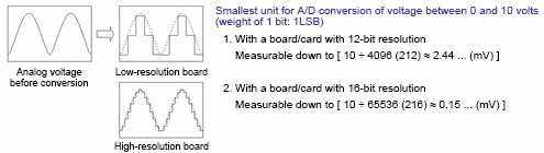
What is resolution?
Resolution refers to the extent of fineness that the analog signal can be digitally represented (approximately). A high resolution means that the voltage range can be finely divided, resulting in a more accurate conversion to digital values.
Let's look at some example considerations for selecting a device with the optimal resolution from among the wide variety of analog I/O devices.
For example, if "measuring between 0°C and 100°C" ...
- Example 1: To measure at units of 1°C
- An accuracy of 1/100 is necessary. A device with 8 bits of resolution (2^8 = 256 segments) is sufficient.
- Example 2: To measure at units of 0.1°C
- An accuracy of 1/1,000 is necessary. A device with 12 bits of resolution (2^12 = 4,096 segments) is required.
- Example 3: To measure at units of 0.01°C
- An accuracy of 1/10,000 is necessary. A device with 16 bits of resolution (2^16 = 65,536 segments) is required.
Analog I/O ADC Resolution (Multi-function DAQ)
Analog I/O DAC Resolution (Multi-function DAQ)
Analog I/O DAC Resolution
What is I/O range?
This is the range of analog voltage or current that can be input or output. A bipolar range covers, for example, from -10 V to +10 V, while a unipolar range would cover only 0 to +10 V. The input/output range should be similar to the output from the sensor and the input to the actuator, or you could choose a device that offers a slightly wider range.
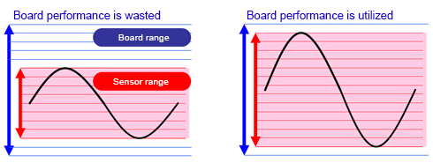
For example, let's assume that we are using a sensor that converts an analog amount to 0 to 5 volts. So, between a device with an input range of 0 to 10 V and one with 0 to 5 V, which is effective? If both have a resolution of 12 bits, the smallest divisible voltage for the 0 to 10 V board is about 2.44 mV (10 ÷ 4096 = about 2.44). With the 0 to 5 V device, the equation becomes 5÷4096, making the smallest divisible voltage 1.22 mV. Because the sensor only outputs 0 to 5 V, the device with an input range of 0 to 5 V will provide the opportunity for finest judgment.
What is gain?
Gain refers to magnification. Some analog input devices are equipped with a function that can amplify the input signal. For example, with an external signal of 0 to 2.5 V, if the input range of an analog input device is 0 to 10 V, amplifying the external signal (the signal being input) by a factor of 4 and then converting the resulting 0 to 10 V signal rather than converting it as is will allow for conversion with higher precision.
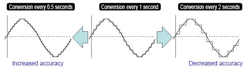
What is the conversion rate (sampling cycle)?
The conversion rate refers to the fineness at which an analog signal can be converted to a digital signal over a specific interval of time. It also shows how much time it takes for digital data to be output as analog data. Higher conversion speeds mean conversions with higher repeatability are possible.
Recommended sampling rate: 10 times the frequency being measured
The first step in measuring an analog signal is to determine the sampling rate (period). A faster sampling rate provides greater accuracy when converting the original signal waveform into a digital signal. However, as the sampling rate increases, the amount of data also increases, resulting in the need for more expensive A/D converters in the analog input interface.
To determine a realistic index, the sampling theorem should be considered first. The sampling theorem specifies the interval at which a continuous analog signal should be sampled into a discrete digital signal. To sample all the frequency components in the original signal accurately, the sampling rate must be at least twice the frequency of the original signal.
For example, accurate sampling of a 1 kHz analog signal requires a sampling rate of at least 2 kHz. Anything less will prevent accurate sampling of the frequency components in the original signal. When sampling at low speeds, a high-speed signal will appear as a folded signal, resulting in aliasing and causing the signal waveform to appear as a lower frequency than the actual original waveform frequency.
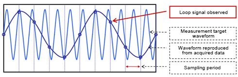
Aliasing is something that can be observed in our daily lives. For example, a propeller rotating at a high speed appears slow because the sampling rate of our eyes and brain cannot keep up with the frequency of the rotating propeller. If aliasing occurs, the sampling result will look significantly different from the actual signal frequency.
Following the sampling theorem should ensure that the frequency components are accurately acquired. In reality, however, the waveform will look jagged and a sufficient amplitude will not be acquired if the sampling rate is only twice the frequency of the original signal. To ensure the signal characteristics are captured accurately, a sampling rate of at least 10 times the frequency of the original signal is recommended. Contec provides various analog input interfaces for specific frequencies.
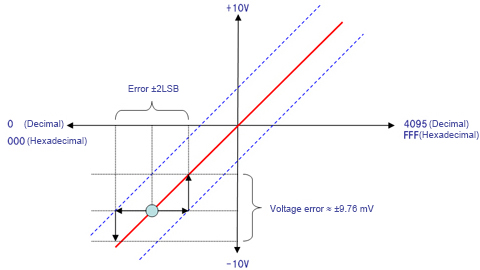
What is conversion accuracy?
Conversion accuracy refers to the error range produced when performing A/D conversions or D/A conversions. Errors are represented in units of 1 LSB. For example, the smallest resoluble unit for an A/D conversion device with a resolution of 12 bits set to an input range of ±10 V is 20 ÷ 4,096 ≈ 4.88 mV (1 LSB). If that A/D conversion board's conversion accuracy is noted as ±2 LSB, it means that there is a possibility that errors produced will be about 4.88 × 2 ≈ ±9.76 mV.
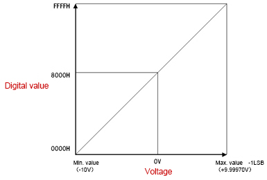
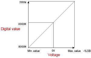
Relationship between binary data and voltage (with 16-bit resolution)
A/D conversion data input from a 16-bit analog input device becomes binary with 16 digits (hexadecimal = 4 digits), and with an analog output device, the D/A conversion data to set is handled with 16-digit binary (hexadecimal = 4 digits). As shown in the following figure, if "0000" is used at "-10 V", then "FFFF" is used at "9.99970 V".
With a 16-bit resolution device, the voltage between -10 V and 0 V can be expressed as 32,768 data segments, where -10 V is "0000H" and 0 V is "8000H." As such, 0 V to 10 V becomes "8000H" to the max. "FFFFH", which must then be expressed as 32,767. For this reason, the maximum value is referred to as "+10 V -1 LSB".
These relationships are the same for any analog I/O device. For example, with analog output, to output a signal externally, "FFFF" is set to a device with 16-bit resolution, but the maximum outputtable voltage is "+10 V -1 LSB".
Abbreviation (unit) meanings
LSB
Abbreviation of least significant bit. Signifies the least significant bit of binary data.
MSB
Abbreviation of most significant bit. Signifies the most significant bit of binary data.
FSR
Abbreviation of full scale range. In the ±10 V range, FSR becomes "20".
Expressing analog values as digital values
Data converted (quantized) through an analog input (A/D conversion) and data set to an analog output (D/A conversion) can be represented using the following unique code systems. The methods for displaying these systems are as follows.
Straight binary
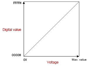
A voltage of 0 V is given a digital value of 0, and the digital value increases in proportion to the increase in voltage. A unipolar form is used.
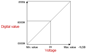
Offset binary
The maximum (lowest) value of negative voltage is given a digital value of 0. In this way, 0 V is assigned a digital value in the middle, and the largest positive voltage value is given the largest digital value. A bipolar form is used.
Complement binary(Two's complement)
To obtain the two's complement, the most significant bit of the offset binary code is reversed. A two's complement expression is an easy-to-use code for calculations on a computer. This data format can be found in bipolar forms.
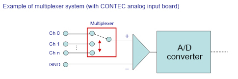
What is the sampling method?
When performing sampling over multiple channels, a multiplexer method using multiplexers (switching units) or a simultaneous sampling method is used.
The multiplexer method performs sampling while switching the multiplexer, meaning that simultaneous conversion of more than one channel is impossible (because time is needed to change between channels).
With the simultaneous sampling method, there are two types: where each channel is equipped with an A/D converter, and where a sample/hold amplifier is equipped. Either type is capable of performing simultaneous conversion over multiple channels.
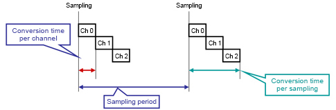
Conversion rates and Nos. of channels
In a system where the analog input channels are switched through a multiplexer method, to perform sampling over multiple channels, the settable sampling period must maintain the following relationship. Conversion rate × sampling cycle ≤ sampling cycle"
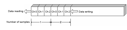
Acquiring data at the same sampling rate
When using an analog input interface to measure multiple signals, the signals from all measured channels are not necessarily sampled at the same rate. If the analog input interface includes enough A/D converters to cover all channels, the analog signals of all channels can be synchronized and sampled at the same rate.
With multiplexer models, however, the channels are switched by the multiplexer and sampled using a single A/D converter. This means that the sampling period for each channel will increase depending on the number of channels, and a gap will be generated in the sampling rate between channels.
|
Simultaneous sampling models
|
Multiplexer models
|
|
|
|
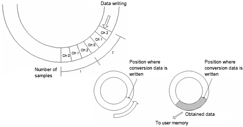
Even with multiplexer-based analog input interfaces, time discrepancies can be eliminated by using a simultaneous sampling function extension accessory. The ATSS-16A can acquire data at the same sampling rate with no time discrepancy by holding the analog input signals of 16 channels simultaneously according to the control signal from the Analog E series.
What is a clock?
A clock indicates the timing at which conversion operations of an analog I/O device can be synchronized. For sampling clocks that determine sampling cycles, the following main methods are used.
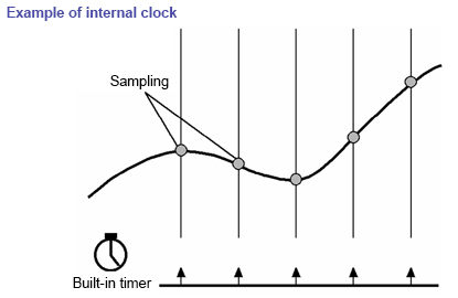
Internal clock
A timer element capable of setting the sampling period is installed in the device. As a clock source, this is a method for performing periodic conversions. Internal clocks are useful for time-series processing at precise and rapid cycles.
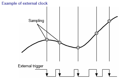
External clock
External clocks can be used for devices equipped with external clock input terminals. Conversion is performed in synchronization with a pulse signal or other signal input from an external source. This method is useful for synchronizing with external devices.
Software clock
A software clock is a method of performing periodic conversions by synchronizing with the system timer on a PC and sending a start command from the software. However, because errors with VisualBasic's timer control and other functions are large, this method is not suitable for systems requiring fast and accurate cycles.
What is a trigger?
A trigger is a source for determining the timing at which to start or stop a conversion. Starting and stopping can both be set independently. The main triggers are as follows.
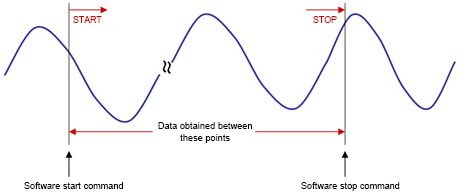
Software trigger
A software trigger starts/stops conversion operations using commands from software.
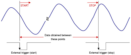
External trigger
An external trigger starts/stops conversion operations using an external signal (digital signal). Conversion operation starts or stops when the pre-set edge movement (rising or falling) is input from the external control signal.
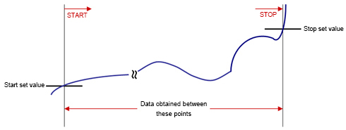
Level comparison (conversion data comparison) trigger
Conversion is started or stopped according to the signal changes for a specified channel. A pre-set comparison level is compared with the magnitude of the analog signal for a specified channel, and if the criteria match, the conversion operation starts/stops.
What is buffer memory?
Buffer memory is where conversion data is temporarily stored. Such memory not only enables fast and high-performance analog input processing but also significantly reduces the load on the computer. Depending on the application, buffer memory can employ either the FIFO method or the ring method.
FIFO method
With the FIFO (First In, First Out) method, converted data is stored in the buffer memory in a first-come, first-served behavior with data written to the buffer memory first being read first (in chronological order). The converted data read from within the memory is delivered sequentially, with reading of the oldest conversion data remaining in the buffer memory always readable. Data that exceeds the FIFO memory capacity will be discarded and not written, and data that has been read will be discarded from the buffer memory.
Ring method
The ring method arranges the storage area in the buffer memory like a ring. Conversion data is written sequentially, and when storing beyond the memory capacity, areas where prior conversion data is stored are overwritten. Ring memory is useful when data is not normally obtained but data near a conversion operation stop due to some event should be obtained. With the ring method, once data is captured, it can be read multiple times before it is overwritten.
Analog I/O Buffer Memory (Multi-function)
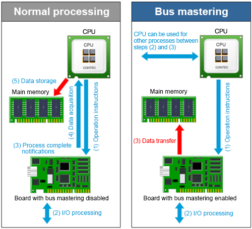
What is bus master transfer function?
This function is a DMA (direct memory access) transfer that uses a PCI bus master function.
- Without applying a load on the PC's CPU, data can be transferred from the device directly to the PC memory at a speed of 80 MB/sec (maximum 133 MB/sec).
- Because the CPU's capacity is not reduced due to data transfer processes and the like, it is able to perform other processes, thus reducing the impact on other applications.
- The necessary settings for input/output are already set to the device, and because the board performs processing based on that information, it's possible to construct a more efficient system than possible with normal input/output processing.
Normal processing
With normal input/output processing, after the CPU reads the data from the device, it stores the information in the main unit's memory. This intermediate CPU cannot be used for other processes. In the following figure, other processes are only possible after (4) and (5) are finished.
Bus mastering
During bus mastering, the CPU instructs bus master processing for the device, allowing data to be sent to the main unit's memory directly from the device (without going through the CPU). In the following figure, other processes can be performed while (2) and (3) are processing.
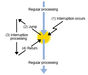
What is interruption?
This function generates priority processing externally by connecting a certain input terminal to an IRQ (interrupt request line) on the computer. By detecting changes in external devices, interruption can be used, for example, in applications that perform specific processing and for processing emergency high-priority external commands, to name a few.
What is current consumption?
To operate a device, power is needed, but current consumption indicates how much current that board consumes. This power is usually supplied from the computers expansion bus connector.
This means that the total maximum current consumption of the board should not be more than the rated power capacity of the computer (the maximum current that can be supplied to the expansion slot).
If the rated power capacity is exceeded, the computer's power supply voltage will be reduced, which could result in such trouble as runaway. For this reason, it's necessary to take appropriate countermeasures, such as extending the computer's slots by using an "expansion unit".
Example: The power supply capacity the computer can supply to the expansion slot is 3.6 A.
- When mounting two 1.2 A external interface boards, the maximum current consumption is as follows:
- 1.2 (A) × 2 (boards) = 2.4 A, which is lower than the power capacity of the computer (3.6 A). [Acceptable]
- When mounting six 0.8 A external interface boards, the maximum current consumption becomes:
- 0.8 (A) × 6 (boards) = 4.8 A, higher than the power capacity of the computer (3.6 A). [Unacceptable]
Types of noise and applicable countermeasures
Noise can generally be categorized into external or internal noise. Unlike with electrical testing, various on-site noises can cause unexpected results that do not conform to theory. In such situations, noise will be the driving factor behind any accuracy deviations.
External noise
- Airborne noise from outside the signal transmission line
- Noise from power system wiring such as motors, or noise from nearby wiring
Internal noise
- Crosstalk between signal lines
- Crosstalk caused by multiplexer switching
- Noise caused by ground loops (earth loops)
Solution
The general rule, particularly when performing measurement, is that noise should not affect the measurement target. To ensure this, it's necessary to take care that impedance, ground levels, and the like, are matching. Familiarizing yourself with solutions is not difficult, but it could be said that failing to consider these solutions can have a large impact. The table below lists some countermeasures against noise.
Hardware
Software
Removing airborne noise
One effective way to remove airborne noise is to connect the analog input interface to the measurement target using a shielded cable. Such cables remove noise because the shielding is grounded through the PC frame, resulting in the cable being grounded with the PC’s power supply.
Eliminating crosstalk between signal lines
Crosstalk is what happens when signal lines interfere with each other, resulting in noise. Using twisted pair cable is an effective way to prevent crosstalk. Contec’s PCB37PS shielded cable includes a signal line and a ground line in a twisted pair, while the PCB96PS includes a twisted pair between differential pairs. The PCC16PS and PCD8PS are also available with coaxial cable signal lines.
Eliminating crosstalk caused by multiplexer switching
The switching of the multiplexer in the analog input interface can affect the signal source waveform. This phenomenon is caused by the charging and discharging of the stray capacitance of the multiplexer via the output impedance of the signal source. With a higher signal source output impedance, the output voltage of the signal source will take longer to return to the desired measurement voltage (known as the settling time).
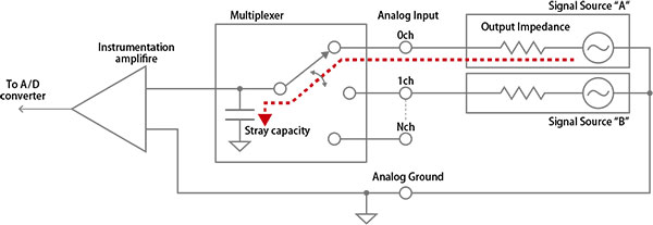 Example input circuit of an analog input interface
The settling time will vary depending on the signal source output impedance. The following is an example of sampling with two channels: signal source A, which has a low output impedance, and signal source B, which has a high output impedance.
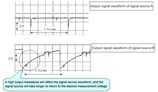
Reducing the signal source output impedance is an effective way to prevent the effects of multiplexer switching. In particular, the signal line should be as short as possible. If the signal line cannot be shortened, or if the target has a high output impedance, multiplexer switching effects can also be prevented by connecting a buffer amplifier with a high input impedance as well as a high-speed, high-precision operational amplifier.
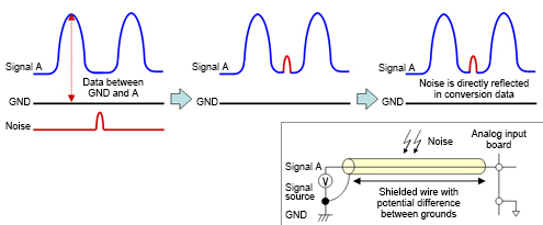
Eliminating errors caused by ground loops (earth loops)
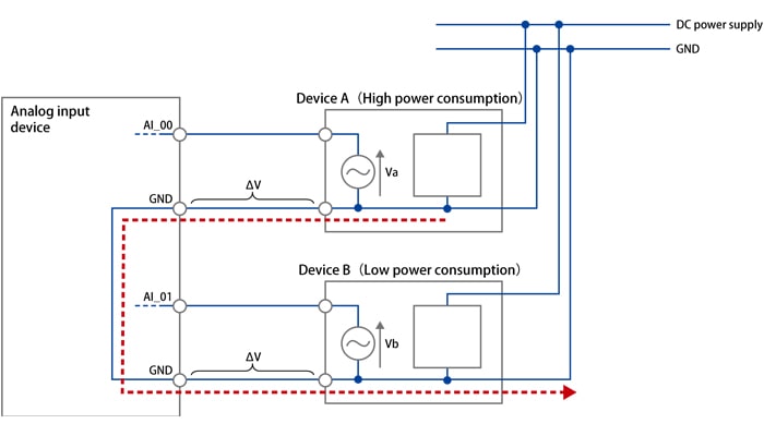
A ground loop, or earth loop, occurs when the ground wiring becomes looped. In a system with multiple connected devices, there may be an electric potential difference between the grounds (GND) of each signal, causing the current to flow in a loop through the ground wiring. When current flows through this ground loop, voltage will be generated depending on the path impedance, and this voltage will appear as a measurement error (noise).
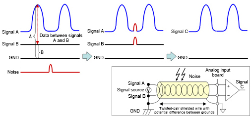
Single-ended input (common mode) is useful when handling a large number of channels, but this input type is affected by ground loops. On the other hand, differential input (differential mode) has half the number of channels of single-ended input and is not affected by ground loops.
Example of errors caused by ground loops
- Single-ended input
- Measurement voltage of AI_00 = Va + ΔV
- Measurement voltage of AI_01 = Vb - ΔV
- With single-ended input, the current flowing through the ground loop causes a measurement error of ΔV.
- Differential input
- Measurement voltage of AI_00 = (Va + ΔV) – ΔV = Va
- Measurement voltage of AI_01 = (Vb – ΔV) – (-ΔV) = Vb
- With differential input, the voltage between the positive (AI_00[+]) and negative (AI_00[-]) terminals can be measured to eliminate errors caused by the ground loop.
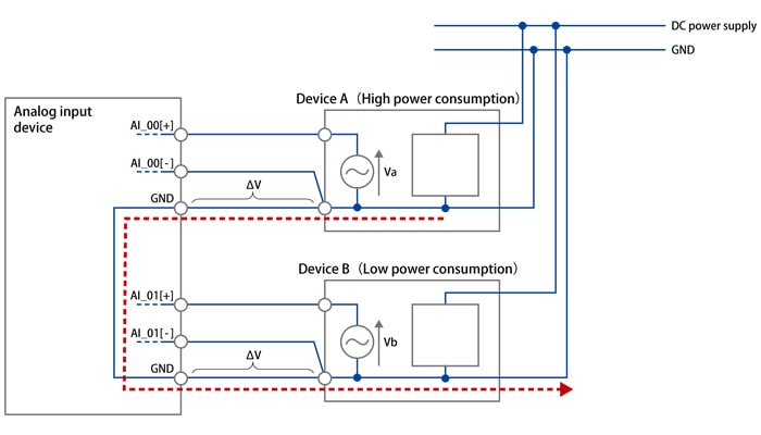
This makes differential input an effective way to prevent ground loop-related errors. If a ground loop is suspected, using bus isolation to cut the ground loop might be useful.